Outsourcing x86 core production to TSMC is just confirming what we already know about Intel’s fabs, they’re garbage.
Intel’s upcoming Meteor Lake architecture marks the company’s inaugural “tile-based”, mobile-exclusive design which is set to release in December. This will also include a ultra-low-power iteration of Meteor Lake, known as “Meteor Lake-U,” with Lunar Lake slated as not being so much a successor / follow-up to Meteor Lake-U as that falls down to Arrow Lake-U.

Lunar Lake should essentially coexist with Arrow Lake-U given that its target market is specifically for ultra-thin devices, but this is clearly speculative.
Leaked slides by Twitter user YuuKi_AnS which have since been removed indicate that the compute tiles for Lunar Lake will instead be leveraging TSMC’s N3B process, a first for Intel, given that Lunar Lake is intended for ultra low power environments between 8-30 watts.

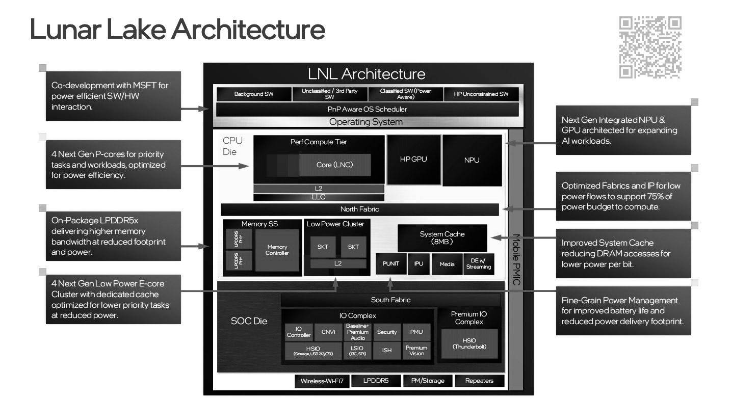
As outlined in the presentation, Intel’s Lunar Lake-MX platform range is set to introduce processors featuring a maximum of eight cores in a 4P + 4E configuration, comprising of four high-performance “Lion Cove” cores paired with four efficient Skymont cores, surprisingly enough there’s no actual inclusion of Intel’s new low-power efficient core which are set to debut with Meteor Lake.
Aside from that, Lunar Lake-MX apparently sports 12MB of cache alongside a maximum of eight Xe2 GPU clusters, and a six-tile NPU 4.0 AI accelerator. The slides also show that Intel developed Lunar Lake in partnership with Microsoft, as it features its invasive Pluton security processing backdoor.
Previously described as leveraging Intel’s own 18A fabrication process, plans have now changed dramatically as it looks like Lunar Lake-MX will be utilizing TSMC’s 3nm process. It certainly bodes well that Intel knows that their own semiconductor simply isn’t up to snuff in terms of actual efficiency.
According to the slides, Intel aims to consolidate the CPU, GPU, and memory controller onto a single tile to minimalize its physical footprint, leaving the remaining components to be integrated into the SoC instead.
Lunar Lake MX will feature two distinct tiles, the CPU & GPU paired with a separate SoC tile.

Additionally, Lunar Lake MX is set to come with LPDDR5X-8533 memory-on-package in configurations of 16GB or 32GB, which aim to further reduce the platform’s footprint and improve overall performance.

According to the information provided in the slides by Intel, the Lunar Lake MX design is expected to reduce the physical footprint by 100 to 250mm2 when compared to conventional designs where memory is located outside the CPU package, the introduction of on-package memory (MoP) also benefits processor efficiency which is the primary goal of the Lunar Lake architecture.

The Lunar Lake MX series is set to support both PCIe Gen5x4 and Gen4x4 interfaces, along with Thunderbolt 4 and up to three USB4 connectors. The chip will feature integrated capabilities for enhanced connectivity, additionally the Xe2-LPG graphics core inside of Lunar Lake features 64 vector engines with support for VVC/H.266 video decoding alongside DisplayPort 1.4, HDMI 2.1 and eDPI 1.4 & 1.5 connection outputs.
If I was being honest, I seriously dislike this tile-based architecture, the entire point of Intel’s endeavors is to be more compact and more modular except the actual diagram itself looks disjointed and needlessly complicated to actually produce in large quantities.

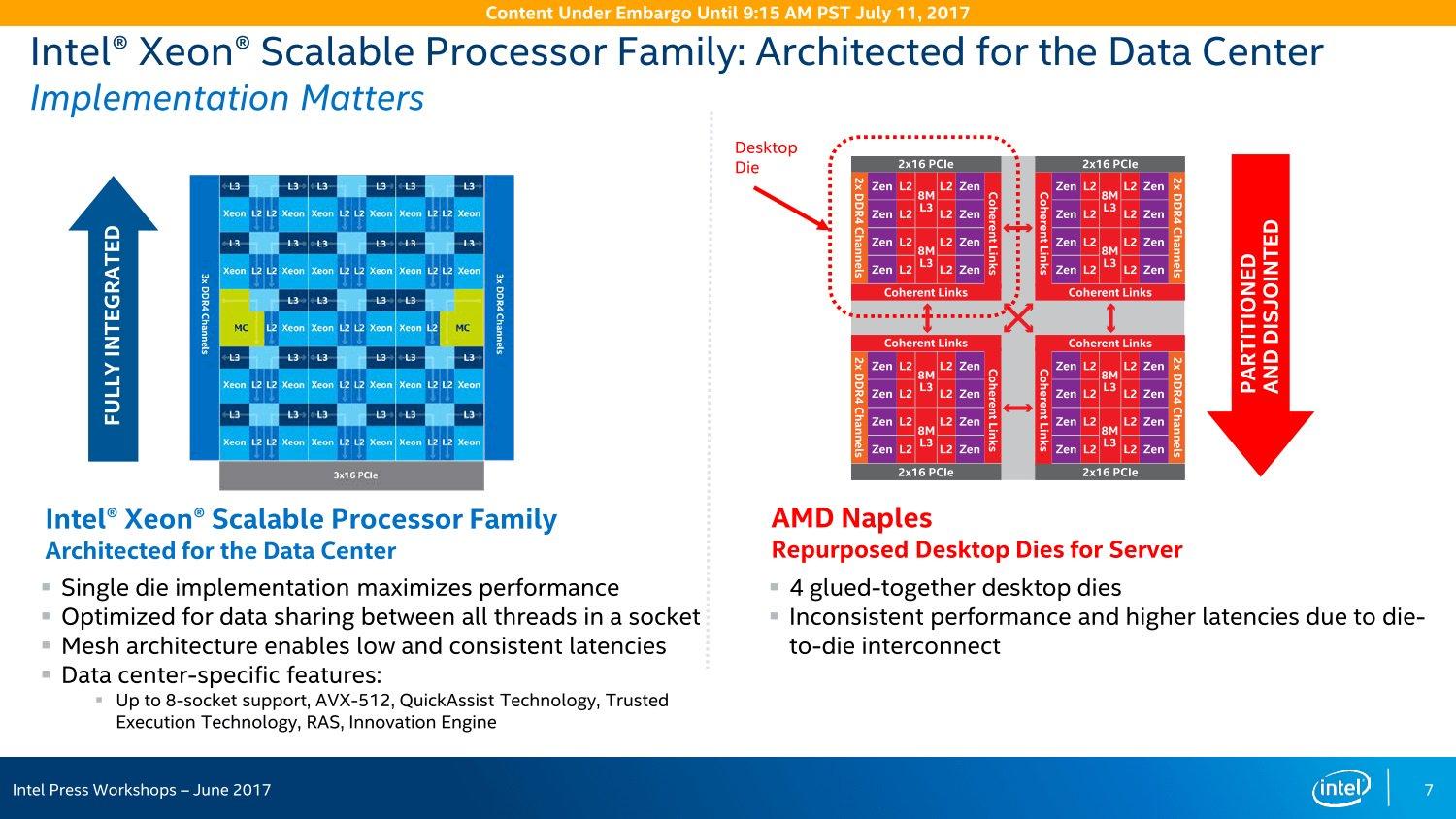
Especially after Intel criticized their main rivals, AMD, in regards to how their enterprise processors consisted of “glued together desktop dies” where Intel’s then monolithic monstrosities were hailed for their superior implementation, whereas AMD’s Zen is a modular chiplet design, Lunar Lake is only modular in the sense that it features a dozen separate modules that are glued together.
The future sure does look bleak for Intel, with their “modular” Sapphire Rapids Xeons getting obliterated by AMD‘s latest crop of EPYC / Threadripper CPUs with a far smaller silicon footprint, their projections for Arrow Lake look woeful, Intel’s own slides projecting a measly 5% increase in single core performance for their 15th Generation Core processors and then there’s this abomination.

TSMC’s founder, Morris Chang at the ripe old age of 92 proclaimed that Intel’s semiconductor wasn’t even a threat to the Taiwanese mafia, and he’d be right. With Intel suffering blow after blow with subsequent delays to their 14nm process, followed by half a decade of waiting for 10nm production to reach acceptable levels, Intel have rebranded their entire semiconductor process and remain adamant that they’re still competitive with industry leaders TSMC.

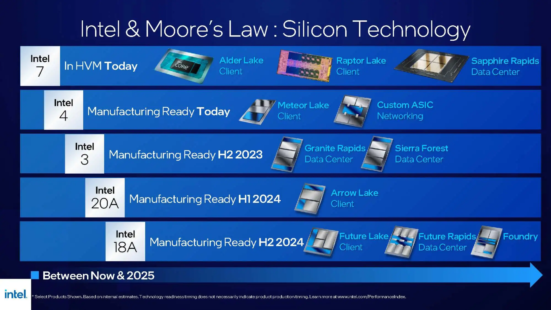
Given how Intel seemingly cannot maintain any sort of proposed roadmap, failing to meet expectations time and time again, they proclaimed that they’re going to be making severe advancements to their fabrication processes, by unleashing four new nodes across six quarters, a feat unheard of and will more than likely fall flat on the faces of Intel shareholders.
Lunar Lake was first mentioned to be utilizing Intel’s 18A (1.8nm) process, but clearly plans have changed given that Lunar Lake MX is slated to utilize TSMC’s N3B processing node and not just for its graphics cluster, Intel’s upcoming Meteor Lake will be built on a mixture of Intel 4 and TSMC 6/5nm processes for the CPU tile, GPU and SoC tiles.
Lunar Lake however is going to be the first time that Intel’s x86 Core architecture is going to be tapped out on a competitor’s foundry, and coincidentally it happens to be specifically for the ultra low power segment, given how Intel 4 is theoretically 7nm, this doesn’t come as much of a surprise that Intel are slowly but surely waving the white flag in terms of their lackluster advancement and progression when it comes to their own foundry.

